Say Goodbye to Wireless Development Headaches! The BN52M-C32 DK (Nordic nRF52832 Module): Your Secret Weapon for Building Exceptional Wireless Products
[TAIWAN, 12th Jun. 2025]
As a senior product development engineer, I know how crucial an intuitive and easy-to-understand guide is for a product's success. After writing the technical article for the BN52H-C40, I'm thrilled to bring you the Development Kit Guide for our other product series, the BN52M-C32 (Nordic nRF52832 module). I hope this article will be the perfect starting point for your MN52M-C32 project.
In this guide, I'll take you deep into the BN52M-C32's key features, including its powerful nRF52832 core, flexible GPIO configuration, optimized low-power modes, and how to easily achieve stable Bluetooth communication. Whether you're developing IoT devices, smart sensors, or wearables, this article provides practical steps and valuable insights to help you turn your ideas into reality. My goal is to enable you to efficiently leverage the full potential of the BN52M-C32 and accelerate your development process.
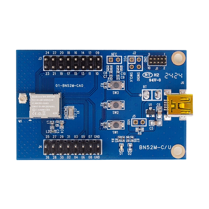
Evaluation Board Package Contents
Package Includes:
BN52M-C32 evaluation board, Type-A to Mini USB cable, 2x5 1.27mm debug cable, and a full-color packaging box.
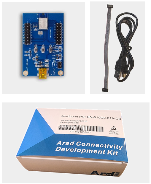
(THE PART NUMBER WILL ALIGN WITH THE ACTUAL PRODUCT)
Component Composition and Function Description
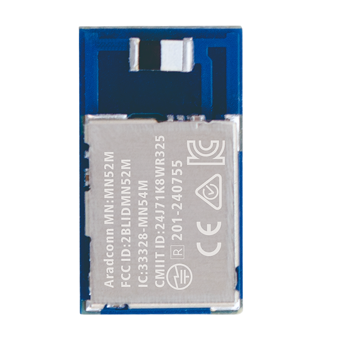
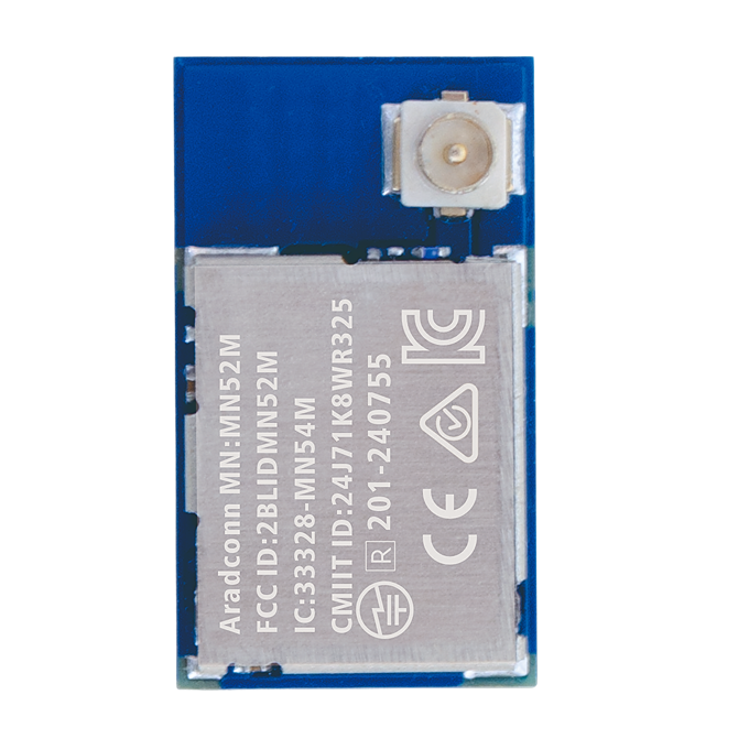
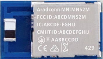
- M1: MN52M-C32 Module (Nordic nRF52832 module)
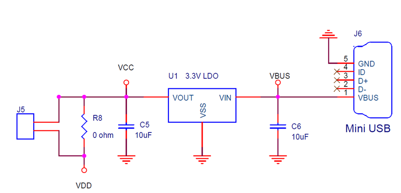
- J6/U1: Mini USB power supply (via U1 LDO) generates 3.3V regulated output.
- J5: To measure the current consumption of the module, please remove R8 and connect a jumper to J5 to measure the current.
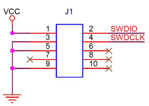
- J1: 2x5 / 1.27mm Debug/Programming Interface, requires an external Nordic debug tool.
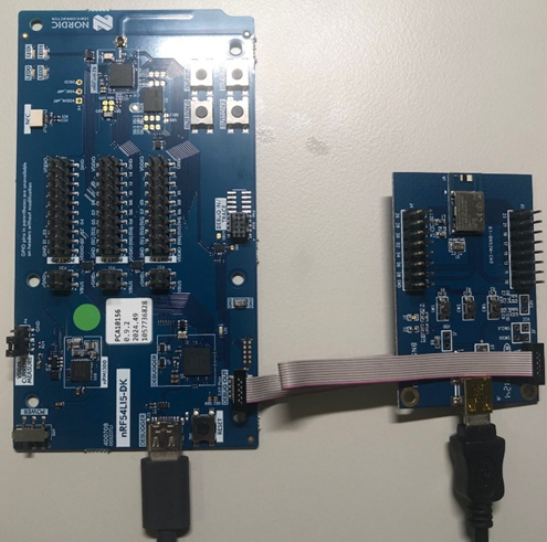
The image shows an example connection between the Nordic nRF54L15-DK and the Arad Connectivity BN52M-C32 DK.
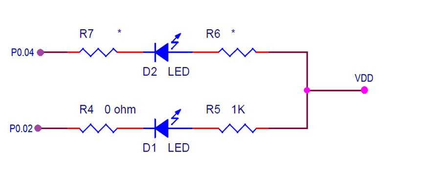
- D1: LED, connected to NRF52832 P0.02/low active.
- D2: LED, connected to NRF52832 P0.04/low active.
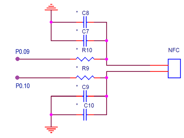
- J3/J4: Full GPIO breakout headers for NRF52832. The symbols represented by J3/J4 are the NRF52832 GPIO symbols.
For example, J3/PIN 1 is 24 = P0.24
For example, J4/PIN 1 is 25 = P0.25
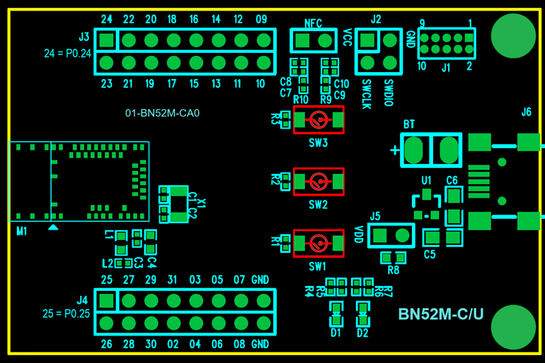
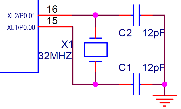
- X1: External 32.768KHz crystal
If additional GPIOs are needed, the LF can be set to the RC internal oscillator, allowing P0.01/P0.00 to be used as GPIOs.
- NFC Matching Capacitors: C7/C8/C9/10/R9/R10 are reserved as NFC antenna matching capacitors
Layout Design Considerations
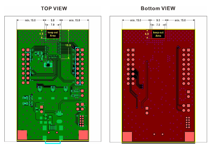
Recommended Module Layout
- Module Placement: Place the module in the center (horizontal direction) of any carrier board edge, with ground planes on both the left and right sides. The antenna end of the module should be aligned with the edge of the carrier board.
- Grounding: Add as many vias as possible around the grounding points between the module and the carrier board, especially at the four corners and the antenna ground area.
- Antenna Keep-out Area: There is a 7 x 4.8 mm keep-out area directly below the antenna. This area needs to be clear on every layer; please do not cover it with ground.
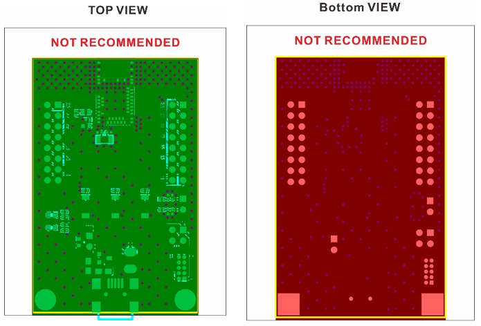
- Incorrect Layout: The keep-out area directly below the module antenna must be reserved and not covered by ground.
Antenna Information:
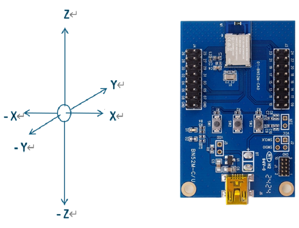
- Antenna Orientation: The antenna's axes are defined by the illustration.
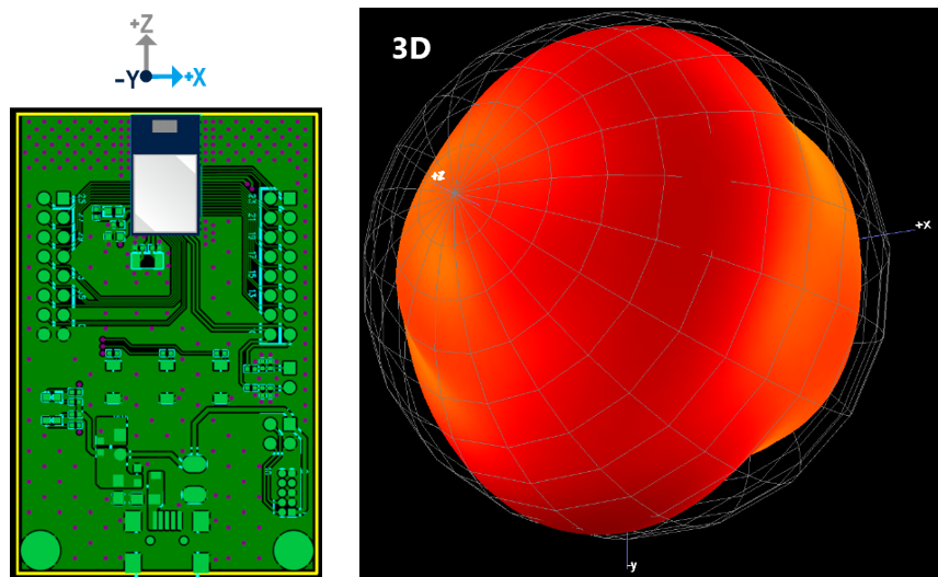
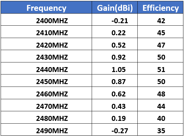
- Antenna Gain and Efficiency:
- Antenna Advantages:
- The radiation pattern is relatively uniform.
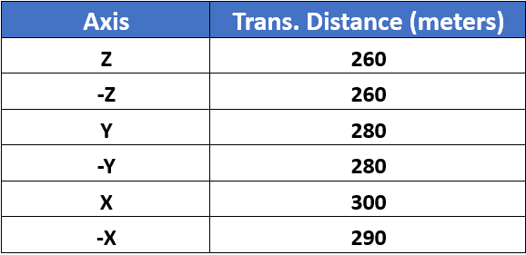
- The measured distances in all six axes are relatively consistent.
- It has the smallest keep-out area, allowing other components (LEDs, switches, connectors) to be placed in areas outside the keep-out zone.
Six-axis Data Transmission Distance result (1 Mbps)
BN52H Chip ANT (MN52H-C40)
Detailed evaluation board test methods and definitions are the same as the MN52H Series Module Range Test Report.
https://www.aradconn.com/news-detail/52Htest/
Edited by Intl. Commercial Development Manager: Mr. Tim Chien
Technical guidance provided by CTO: Mr. Venson Laio