In-Depth Overview of Arad's BN52H-C40 (Nordic nRF52840 Module): A High-Efficiency BLE Evaluation Board for Wireless Applications
[TAIWAN, 06th Jun. 2025]
In the rapidly growing IoT and wireless communication markets, having a reliable, high-performance, and integration-friendly BLE platform is crucial. Arad Connectivity’s BN52H-C40 Evaluation Board, powered by the Nordic nRF52840 SoC, features an integrated high-efficiency chip antenna and comprehensive I/O expansion interfaces. It serves not only as an ideal solution for development and testing but also as a crucial bridge to mass production.This evaluation board overview is designed to help users quickly grasp the module’s key specifications and essential design considerations, including:
- Circuit configuration
- Power supply switching
- GPIO pin header design
- RF performance
- Module layout logic
By understanding the core advantages of the BN52H-C40, developers can accelerate their workflow and enhance product integration efficiency.
Evaluation Board Package Contents
Package Includes:
BN52H-C40 evaluation board, Type-A to Mini USB cable, 2x5 1.27mm debug cable, and a full-color packaging box.
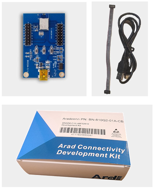
(THE PART NUMBER WILL ALIGN WITH THE ACTUAL PRODUCT)
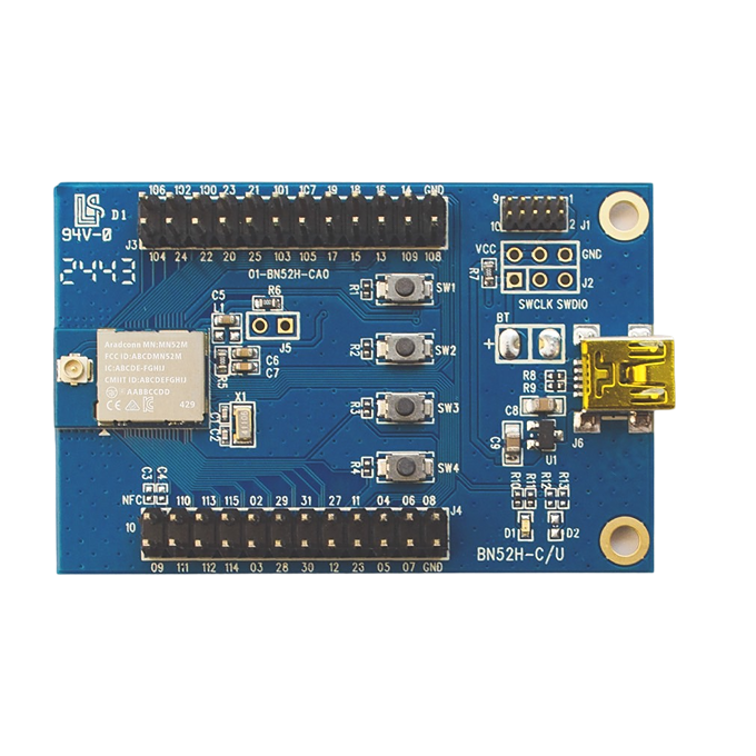
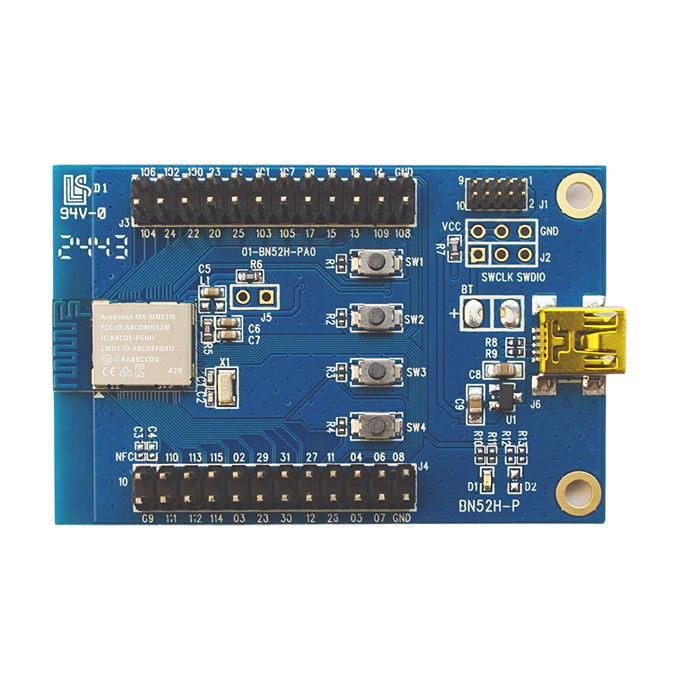
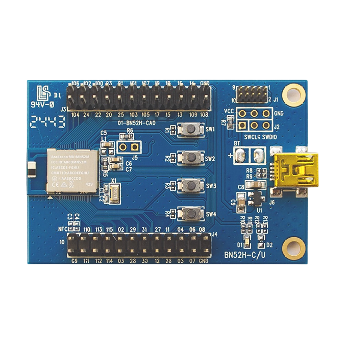
Component Composition and Function Description
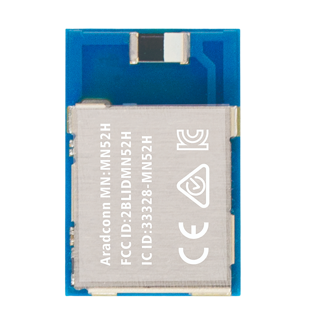
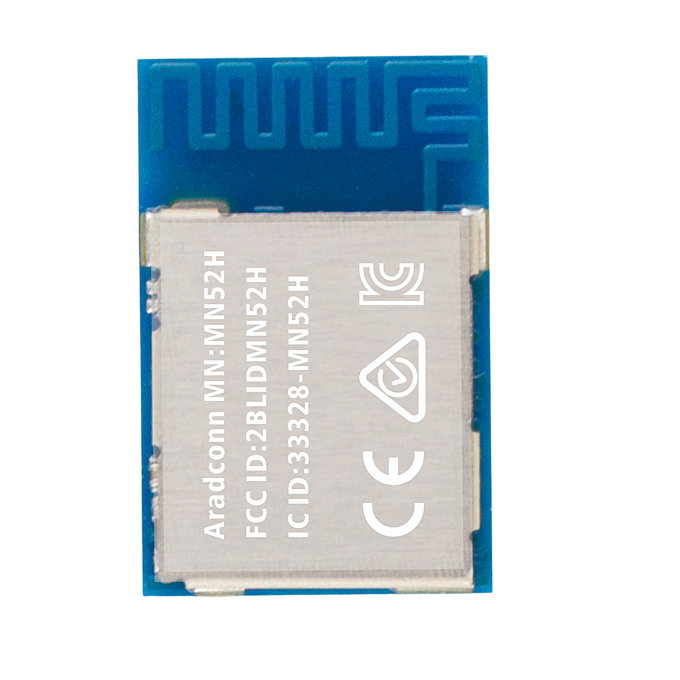
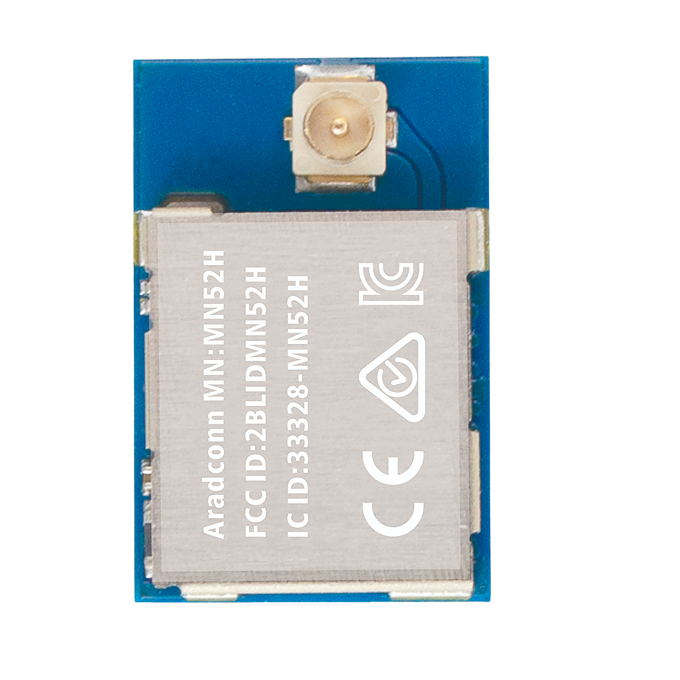
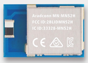
- M1: MN52H-C40 Module (Nordic nRF52840 module)
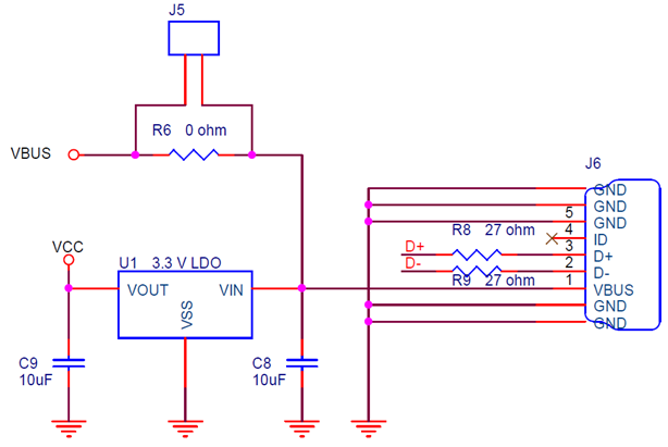
- J6/U1: Mini USB power supply (via U1 LDO) generates 3.3V regulated output.
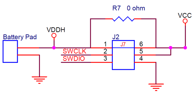
- J7: PIN1/PIN6 of J2 (J7)
To measure the current consumption of the module, please remove R7 and connect a jumper to J7 to measure the current.
- J5: to measure the VBUS current consumption, please remove R6 and connect a jumper to J5 to measure the current.
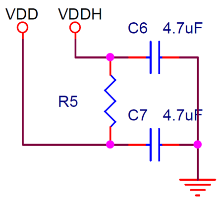
- Power Supply Note: The default module power configuration is 3.3V = VDD = VDDH.
If you need to supply power via VDDH input, please remove R5 and set the desired VDD voltage through the firmware.
- J1: 2x5 / 1.27mm Debug/Programming Interface, requires an external Nordic debug tool.

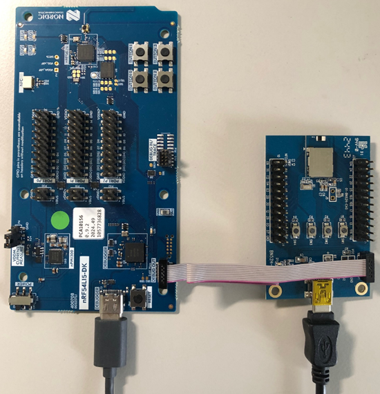
The image shows an example connection between the Nordic nRF54L15-DK and the Arad Connectivity BN52H-C40 DK.
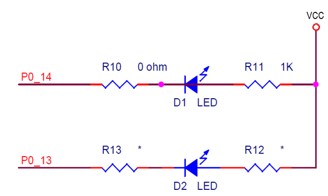
- D1: LED, connected to NRF52840 P0.14 / low active.
- D2: LED, connected to NRF52840 P0.13 / low active.
- J3/J4: Full GPIO breakout headers for NRF52840. The symbols represented by J3/J4 are the NRF52840 GPIO symbols.
For example, J3/PIN 1 is 106 = P1.06.
For example, J4/PIN 1 is 10 = P0.10.
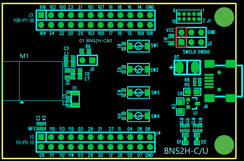
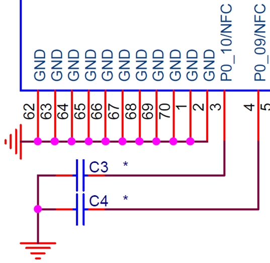
- X1: External 32.768KHz crystal
If additional GPIOs are needed, the LF can be set to the RC internal oscillator, allowing P0.01/P0.00 to be used as GPIOs.

- NFC Matching Capacitors: C3/C4 are reserved as NFC antenna matching capacitors
Layout Design Considerations
Recommended Module Layout
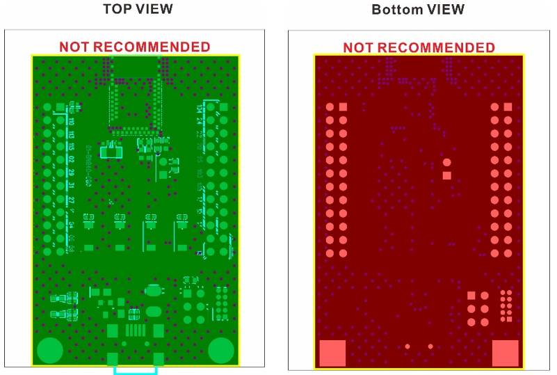
- Module Placement: Place the module in the center (horizontal direction) of any carrier board edge, with ground planes on both the left and right sides. The antenna end of the module should be aligned with the edge of the carrier board.
- Grounding: Add as many vias as possible around the grounding points between the module and the carrier board, especially at the four corners and the antenna ground area.
- Antenna Keep-out Area: There is an 8.1 x 4.4 mm keep-out area directly below the antenna. This area needs to be clear on every layer; please do not cover it with ground.
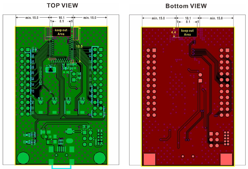
- Incorrect Layout: The keep-out area directly below the module antenna must be reserved and not covered by ground.
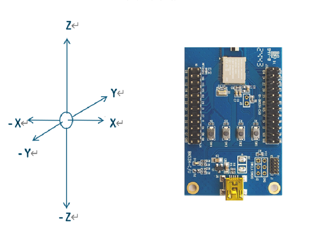
Antenna Information:
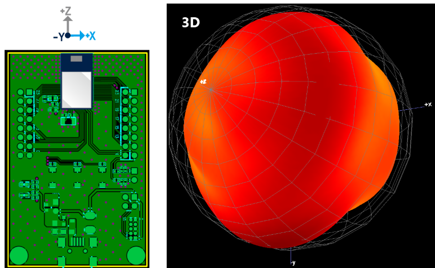
- Antenna Orientation: The antenna's axes are defined by the illustration.
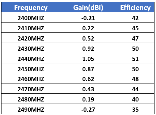
- Antenna Gain and Efficiency:
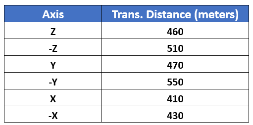
- Antenna Advantages: The radiation pattern is relatively uniform, and the measured distances in all six axes are relatively consistent. It has the smallest keep-out area, allowing other components (LEDs, switches, connectors) to be placed in areas outside the keep-out zone.
Six-axis Data Transmission Distance result (1 Mbps)
BN52H Chip ANT (MN52H-C40)
Detailed evaluation board test methods and definitions can be found in the MN52H Series Module Range Test Report.
https://www.aradconn.com/news-detail/52Htest/
Edited by Intl. Commercial Development Manager: Mr. Tim Chien
Technical guidance provided by CTO: Mr. Venson Laio